|
|
SERIAL ATA-PHY
LC15-TR02 is a stand-alone Serial ATA physical layer that is designed based on SATA standard. This PHY is a 1.5Gbps transceiver that provides very high-speed data transmission. The SATA PHY parameters are compliant with the Serial ATA Gen1 revision 1.0 specification. It is also capable of data transmission of 3Gb/s Gen2 SATA. The parallel interface to link layer is based on SAPIS specification to provide 10bit interface in both rising and falling edges of clock. It also accepts two 10bit 8b/10b encoded transmit characters in parallel and latches them on the rising edge of TBC. Internal endec may be selected to do the 8/10bit encoding on 8bit data. The serialized data is transmitted onto the TXP/TXN differential outputs at a baud rate twenty times of the TBC frequency. It also samples serial received data on the RXP/RXN differential inputs, recovers the clock and data, de-serializes it into one (SAPIS) or two 10bit receive characters in parallel. The recovered clock is sent out at one twentieth of the incoming data rate. The receiver includes the squelch detector, out of band (OOB) signal detector, and is capable of detecting "Comma" characters. This transceiver contains on-chip PLLs circuitry for synthesis of the transmitting clock and extraction of the clock from the received serial stream. The transmit PLL is also responsible for Link layer reference clock generation (ASIC_CK). The circuit requires only one external component. Additional on-chip serial port interface is employed to adjust the performance of certain blocks.
FEATURES
GENERAL
- Serial ATA rev1 compliant- Gen1 physical layer. Bit rate ready for 3Gb/s Gen2.
- Frequency synthesizer for ASIC clock generation of 150 or 300MHz.
- Built in transmission PLL circuits.
- Parallel 10b interface based on SAPIS specification Rev. 0.9
- Optional 20bit transmit data (two 10bit 8b/10b encoded characters).
- Optional internal 8/10bit endec.
- Read/write serial port interface to program the transmission and receive characteristics.
- Power Monitor for glitch free Power Off/On cycles.
- Power management modes: PARTIAL, SLUMBER , STOP.
- Low Power consumption, less than TBDmW.
- Device status to Link layer.
TRANSMITTER
- Transmission speed of 1.5Gb/s for Gen1 and 3Gb/s for Gen2 differential NRZ serial stream.
- Provides a 100 Ohm matched differential termination at the transmitter.
- Serialize 10bit or 20bit parallel input from the Link layer.
- Spread spectrum modulation for TX PLL clock with +0/-0.5% slow frequency variation, over a 33.33 us up/down triangular wave period.
- DC or AC coupled to the SATA cable.
- Far-End and Near-End analog loop back.
RECEIVER
- 1.5Gb/sec for Gen1 and 3Gb/sec for Gen2 differential NRZ serial stream.
- 100 Ohm matched differential termination at the receiver.
- Extract data and clock from the serial stream.
- De-serialize the serial stream into 10bit or 20bit parallel data.
- Detection of K28.5 comma character to provide word aligned 10bit or 20bit parallel output.
- Squelch detector
- OOB signal detection for COMWAKE, COMINIT/COMRESET.
- DC or AC coupled to the SATA cable.
- Built in Clock Recovery PLL for de-serializer and decoder circuits.
SYSTEM OVERVIEW 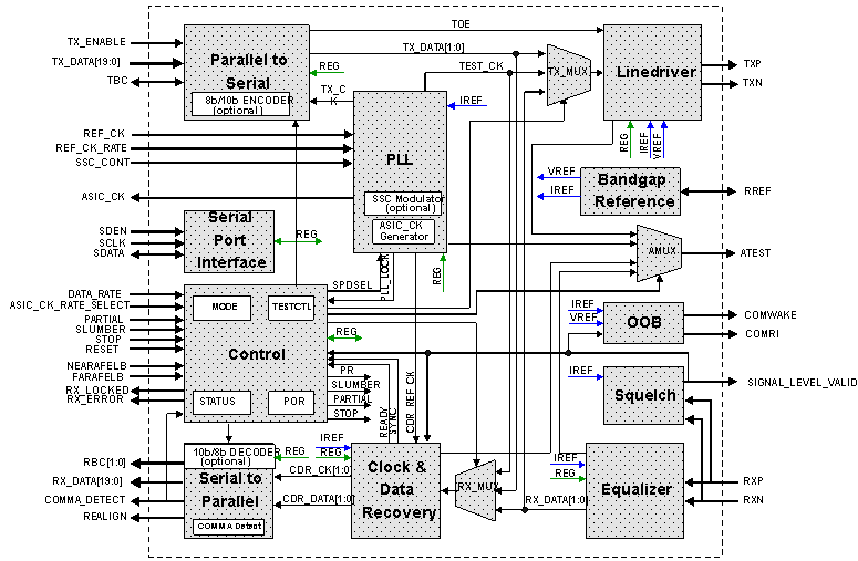
BACK
|
|

|